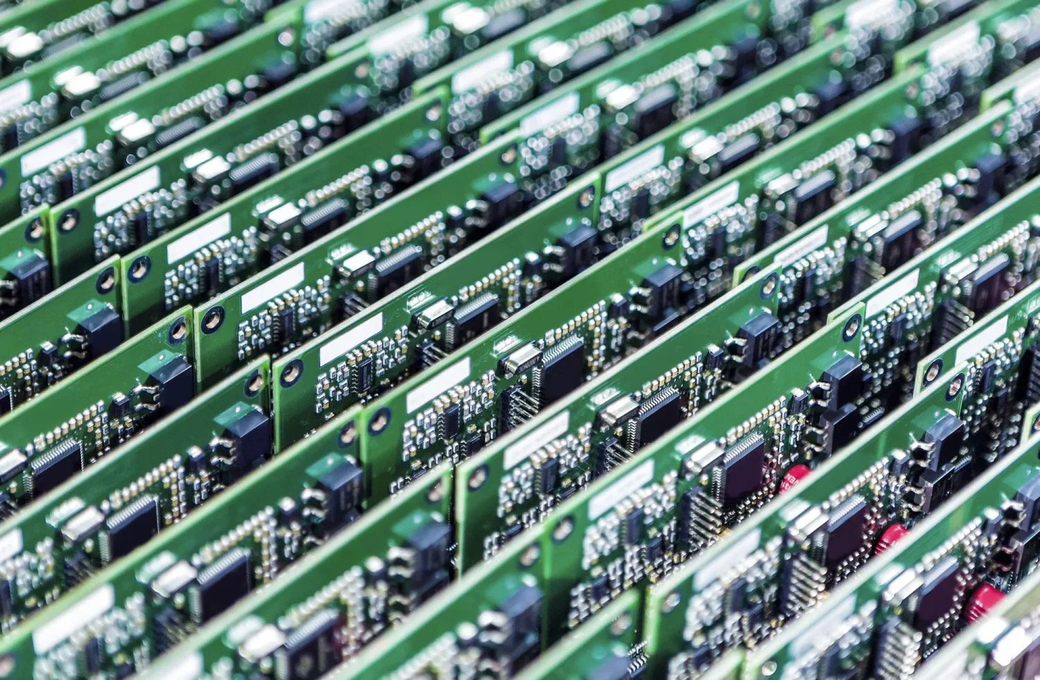
The PCB is the core of every electronic device. Plates connect electronic components by creating pathways through copper pads and connecting wires. That is why the process of assembling a board is one of the most intriguing concepts in electronics. Thus, PCB fabrication is a very complex process.
If you want your board to be properly assembled, it is important that you understand the basics of this process. Remember that PCBs are the basis that allows components to communicate with each other. So learn all about the steps used in the modern PCB assembly process as well as many other information about the board.
1. Basics of PCB design
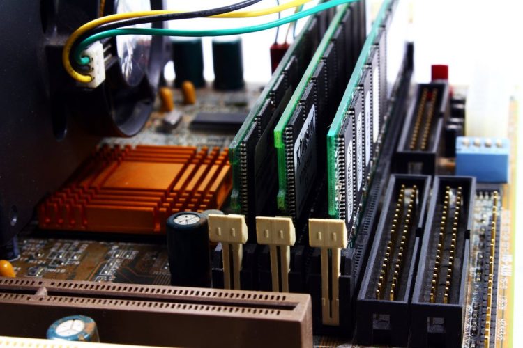
At the beginning of this process is always the most basic unit of PCBs. It is a base consisting of several layers. Each of them plays an important role in the functionality of the final PCB. This includes the substrate, as the base material. Copper is a thin layer that is added to each side of the plate, depending on whether it is one-sided or two-sided. It also contains a soldering mask located on top of the layer. It is this mask that gives the PCB its characteristic green color.
We must mention that it insulates the traces of copper and keeps everything in its place. We must not forget the holes that are in the mask, and they are used to attach components to the plate. This is the most important step in production. Screen printing is the last layer on the board and helps to indicate the functions of the components. The layers are mostly the same in all PCBs except the substrate. The substrate depends on price, flexibility and similar factors. If you want to find out more check this.
2. Through-hole technology
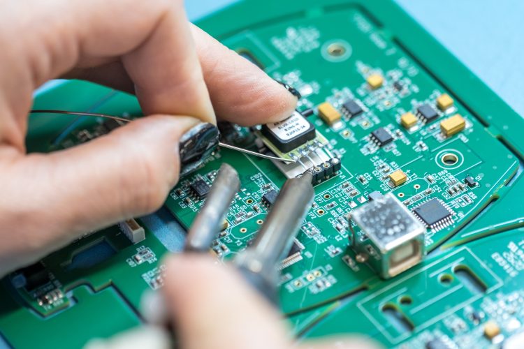
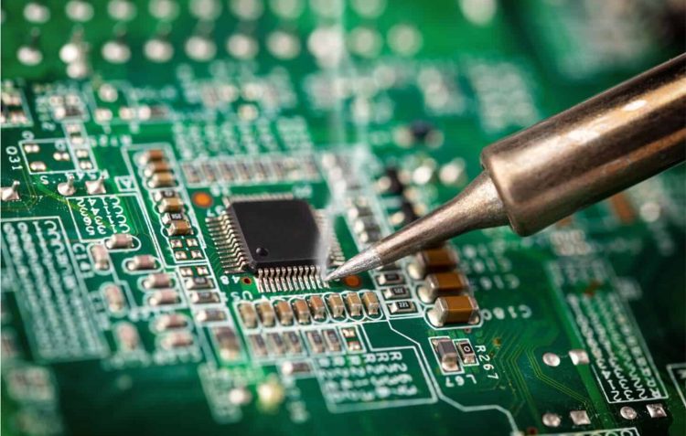
It is an ideal choice for printed circuit boards with wires or wires that pass through the holes in the board. It is an equally good choice for PCBs with large components. You can learn this PCB technology in just a few steps. Depending on the design requirements, the technician assembles the parts on the boards. It is necessary that each component corresponds to the intended position. Otherwise the PCB will not work properly. This is followed by control. It is necessary to determine that all parts are installed correctly. If an error is observed in assembling or setting up the components, there is still time to correct any imperfections. Then, soldering on the motherboard follows and this is done by wave soldering. This means that hot soldering fluid is used. Thanks to it, the PCB assembly is fixed. This technique can be performed manually or with a selective solder.
Holes with a hole are often limited to larger components due to the intersection between the upper and lower surface. Electromechanical relays and plug connectors are also made through holes. Technicians at this stage generally opt for a larger surface placement opening unless the panel is designed for higher speeds or high frequencies. In this case, surface mounting is required. After the components are put in place, an inspection follows, followed by a solder paste over the hot liquid. When this phase is over, the plate is cooled in a controlled environment and returned to normal. This avoids the shock phase. After everything is perfect, the plate is examined to determine the correctness of the components. Irregularities can often be determined only by visual inspection. However, optical and X-ray examinations are usually combined to achieve greater accuracy. If a design problem is detected, the problem must be solved automatically until the other panels have gone through the process.
3. Types of PCBs
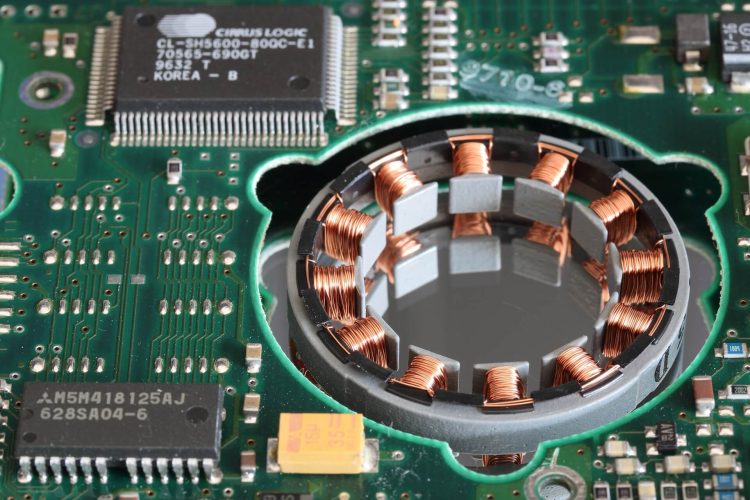
There are three basic types of board and these are solid PCBs, flexible PCBs and metal core PCBs. The first type of board is characterized by a rigid core that gives the board thickness. This PCB base is not flexible and consists of several materials. It is mostly fiberglass or epoxy if it is a cheaper option. Cheaper materials are much less durable than fiberglass.
Unlike this type of board, flexible PCBs are much more flexible. The material used is mainly flexible plastic. A PCB with a metal core is an alternative to flexible boards. It also spreads heat better than other types, which contributes to heat savings and protection of the plate components.
4. Types of inspection
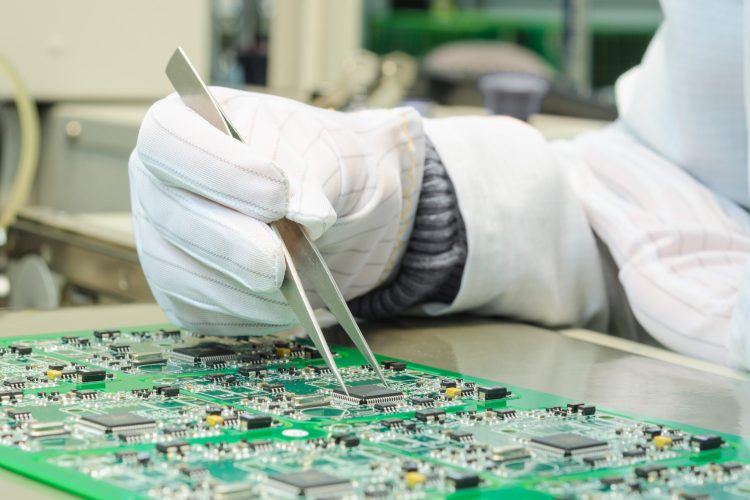
In the previous part of the text, we mentioned quality control as a regular step in the process of manufacturing PCBs, but there are several types of testing. These are manual checks that are still present despite the development of automated and smart production. It is used in the production of smaller series by designers. However, applying this method to a larger number of boards is not a good idea because it is more practical. Looking at too many plates for too long leads to optical fatigue resulting in less accurate inspection. In the case of larger batches, automatic optical inspection is chosen as the appropriate method. During the inspection, AOI machines are used, which are arranged at different angles in order to cover all solder joints.
The machine recognizes defects in a very short time, because it performs inspections at high speed, which allows the processing of large quantities of PCBs. X-ray inspection is another method of inspection and is used to examine complex and layered PCBs. Of course, it all depends on the PCB’s standard. The last step of the inspection is to test the work. In this way, their correctness is checked. If the boards require programming or calibration, a few more steps need to be included to test for correctness. Thanks to regular checks, all errors can be found and eliminated in time, and thus designers save time, work and materials.
Conclusion:
Electronics are an integral part of our lives, and the heart of every device is the PCB. They are much more than miniature ornaments. Its functions range from simple to complex, and as you may have noticed, this process is not difficult to understand.